声波扫描显微镜
价格:电议
地区:四川省
电 话:028-87335465
手 机:13458609644
图文详情
产品属性
相关推荐
Scanning Acoustic Microscopy, commonly referred to as SAM or SAT (Scanning Acoustic Tomography) is unparalleled in its ability to spot delaminations, cracks and other anomalies non-destructively. Not only does acoustic microscopy detect the failures but it also can provide the specific location of the problem. Sonix SAMs high resolution images and advanced diagnostic tools are used to:
The Sonix Advantage
The purchase of a Scanning Acoustic Microscope (SAM) is a major decision. A primary consideration in the purchase process is the system must be capable of producing the desired benefits for years to come. In a world of constant technological advances, knowing the "true" architecture of a product is the key to reducing obsolescence, allowing for cost-effective upgrades, and reducing down time through serviceability. Sonix utilizes state-of-the-art technology that ensures your investment meets current and future expectations. Below is a listing of our line of SAM systems currently available for a variety of semiconductor inspection needs.
PRODUCTS
ECHO:
New from Sonix only-make set up and testing EASY by using the unique interactive touch screen and joystick controls right at the tool.
Echo-The universal inspection tool for production, failure analysis and development.
Sonix ECHO can detect defects as small as 0.05 micron and is an excellent tool for bump detection,stacked die inspection, complex Flipchip inspection and more traditonal plastic packages.
SonixTM transducers range in frequency from 10MHz through 300MHz and are designed to address all types of applications and materials.
Other Key Features
Reduced tank height (for improved ergonomics)
Maximum 360° Visibility (for ease of use)
Salanted tank bottom ( for complete draining)
Touch screen and joystick (for ease of use)
Compact and robust system Design ( for low maintenance)
Welded unibody frame (for improved platform stability)
Simultaneous pulse echo and through transmission options (quick defect detection)
Large scan area (for multiple trays or larger samples)
Transducer based Z-axis (moves transducer instead of tray fixture)
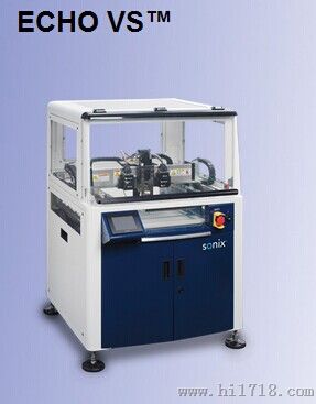
To identify the smallest and most subtle defects in leading-edge packaged microelectronic applications, ECHO VS includes standard features such as heated water for optimum acoustic coupling, Flexible TAMI for efficient capture of the most useful data, Waveform Averaging for an improved signal-to-noise ratio, ICEBERG for improved image quality and MFCI for enhanced image quality in the most demanding applications. ECHO VS is the ultimate scanning acoustic solution for molded flip chip, CSP, MCM, stacked die, MUF and other advanced packaging technologies.
Product Details:
This industry-leading scanning acoustic microscope provides a universal inspection tool for packaged semiconductor development, production and failure analysis. With the ability to detect air defects as thin 0.05 micron and spatially resolve defects down to 10 microns, the ECHO is perfect for bump detection, stacked die (3D packaging) inspection, complex flip chip inspection and more traditional plastic packages.
Vision
Advanced Acoustic Microscopy for stacked die Flip Chips and Bumped Die.