
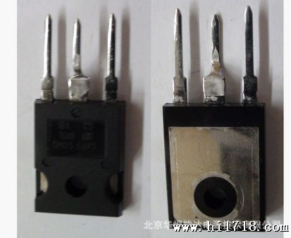
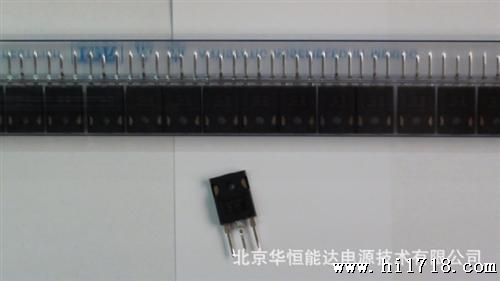
原装库存G4PF50WD场效应管
价格:电议
地区:北京
电 话:86 010 62980032
传 真:86 010 82758336
图文详情
产品属性
相关推荐
IRG4PF50WD
INSULATED GATE BIPOLAR TRANSISTOR WITH
ULTRAFAST SOFT RECOVERY DIODE
Features
E
G
n-channel
C
• Optimized for use in Welding and Switch-Mode
Power Supply applications
• Industry benchmark switching losses improve
efficiency of all power supply topologies
• 50% reduction of Eoff parameter
• Low IGBT conduction losses
• Latest technology IGBT design offers tighter
parameter distribution coupled with
exceptional reliability
• IGBT co-packaged with HEXFREDTM ultrafast,
ultra-soft-recovery anti-parallel diodes for use in
bridge configurations
• Industry standard TO-247AC package
Benefits
PD- 91788
Parameter Min. Typ. Max. Units
RqJC Junction-to-Case - IGBT ––– ––– 0.64
RqJC Junction-to-Case - Diode ––– ––– 0.83 °C/W
RqCS Case-to-Sink, flat, greased surface ––– 0.24 –––
RqJA Junction-to-Ambient, typical socket mount ––– ––– 40
Wt Weight ––– 6 (0.21) ––– g (oz)
Thermal Resistance
• Lower switching losses allow more cost-effective
operation and hence efficient replacement of larger-die
MOSFETs up to 100kHz
• HEXFREDTM diodes optimized for performance with IGBTs.
Minimized recovery characteristics reduce noise, EMI and
switching losses
www.irf.com1
TO-247AC
VCES = 900V
VCE(on) typ. = 2.25V
@VGE = 15V, IC = 28A
Parameter Max. Units
VCES Collector-to-Emitter Breakdown Voltage 900 V
IC @ TC = 25°C Continuous Collector Current 51
IC @ TC = 100°C Continuous Collector Current 28 A
ICM Pulsed Collector Current 204
ILM Clamped Inductive Load Current 204
IF @ TC = 100°C Diode Continuous Forward Current 16
IFM Diode Maximum Forward Current 204
VGE Gate-to-Emitter Voltage ± 20 V
PD @ TC = 25°C Maximum Power Dissipation 200
PD @ TC = 100°C Maximum Power Dissipation 78
TJ Operating Junction and -55 to + 150
TSTG Storage Temperature Range
Soldering Temperature, for 10 seconds 300 (0.063 in. (1.6mm) from case )
°C
Mounting torque, 6-32 or M3 screw. 10 lbf•in (1.1N•m)
Absolute Maximum Ratings
W
IRG4PF50WD
2www.irf.com
Parameter Min. Typ. Max. Units Conditions
V(BR)CES Collector-to-Emitter Breakdown Voltage 900 — — V VGE = 0V, IC = 250μA
DV(BR)CES/DTJ Temperature Coeff. of Breakdown Voltage — 0.295 — V/°C VGE = 0V, IC = 3.5mA
VCE(on) Collector-to-Emitter Saturation Voltage — 2.25 2.7 IC = 28A VGE = 15V
— 2.74 — V IC = 60A See Fig. 2, 5
— 2.12 — IC = 28A, TJ = 150°C
VGE(th) Gate Threshold Voltage 3.0 — 6.0 VCE = VGE, IC = 250μA
DVGE(th)/DTJ Temperature Coeff. of Threshold Voltage — -13 — mV/°C VCE = VGE, IC = 250μA
gfe Forward Transconductance 26 39 — S VCE = 50V, IC = 28A
ICES Zero Gate Voltage Collector Current — — 500 μA VGE = 0V, VCE = 900V
— — 2.0 VGE = 0V, VCE = 10V, TJ = 25°C
— — 6.5 mA VGE = 0V, VCE = 900V, TJ = 150°C
VFM Diode Forward Voltage Drop — 2.5 3.5 V IC = 16A See Fig. 13
— 2.1 3.0 IC = 16A, TJ = 150°C
IGES Gate-to-Emitter Leakage Current — — ±100 nA VGE = ±20V
Parameter Min. Typ. Max. Units Conditions
Qg Total Gate Charge (turn-on) — 160 240 IC = 28A
Qge Gate - Emitter Charge (turn-on) — 19 29 nC VCC = 400V See Fig. 8
Qgc Gate - Collector Charge (turn-on) — 53 80 VGE = 15V
td(on) Turn-On Delay Time — 71 — TJ = 25°C
tr Rise Time — 50 — ns IC = 28A, VCC = 720V
td(off) Turn-Off Delay Time — 150 220 VGE = 15V, RG = 5.0W
tf Fall Time — 110 170 Energy losses include "tail" and
Eon Turn-On Switching Loss — 2.63 — diode reverse recovery.
Eoff Turn-Off Switching Loss — 1.34 — mJ See Fig. 9, 10, 18
Ets Total Switching Loss — 3.97 5.3
td(on) Turn-On Delay Time — 69 — TJ = 150°C, See Fig. 11, 18
tr Rise Time — 52 — ns IC = 28A, VCC = 720V
td(off) Turn-Off Delay Time — 270 — VGE = 15V, RG = 5.0W
tf Fall Time — 190 — Energy losses include "tail" and
Ets Total Switching Loss — 6.0 — mJ diode reverse recovery.
LE Internal Emitter Inductance — 13 — nH Measured 5mm from package
Cies Input Capacitance — 3300 — VGE = 0V
Coes Output Capacitance — 200 — pF VCC = 30V See Fig. 7
Cres Reverse Transfer Capacitance — 45 — ƒ = 1.0MHz
trr Diode Reverse Recovery Time — 90 135 ns TJ = 25°C See Fig.
— 164 245 TJ = 125°C 14 IF = 16A
Irr Diode Peak Reverse Recovery Current — 5.8 10 A TJ = 25°C See Fig.
— 8.3 15 TJ = 125°C 15 VR = 200V
Qrr Diode Reverse Recovery Charge — 260 675 nC TJ = 25°C See Fig.
— TJ = 125°C 16 di/dt = 200A/μs
di(rec)M/dt Diode Peak Rate of Fall of Recovery — 120 — A/μs TJ = 25°C See Fig.
During tb — 76 — TJ
= 125°C 17
Switching Characteristics @ TJ = 25°C (unless otherwise specified)
Electrical Characteristics @ TJ = 25°C (unless otherwise specified)
IRG4PF50WD
www.irf.com3
0.1 1 10 100
0
10
20
30
40
f, Frequency (KHz)
LOAD CURRENT (A)
Fig. 1 - Typical Load Current vs. Frequency
(Load Current = IRMS of fundamental)
For both:
Duty cycle: 50%
T = 125°C
T = 90°C
Gate d rive as specified
sink
J
Power Dissipation = W
60% o f rated
voltage
I
Ideal d iodes
Square wave:
40
Fig. 2 - Typical Output Characteristics Fig. 3 - Typical Transfer Characteristics
1
10
100
1000
1 10
V , Collector-to-Emitter Voltage (V)
I , Collector-to-Emitter Current (A)
CE
C
V = 15V
20μs PULSE WIDTH
GE
TJ = 25 ° C
TJ = 150 ° C
1
10
100
1000
5 6 7 8 9 10
V , Gate-to-Emitter Voltage (V)
I , Collector-to-Emitter Current (A)
GE
C
V = 50V
5μs PULSE WIDTH
CC
TJ = 25 ° C
TJ = 150 ° C
IRG4PF50WD
4www.irf.com
Fig. 6 - Maximum Effective Transient Thermal Impedance, Junction-to-Case
Fig. 5 - Collector-to-Emitter Voltage vs.
Junction Temperature
Fig. 4 - Maximum Collector Current vs. Case
Temperature
125 150
0
10
20
30
40
50
60
T , Case Temperature ( C)
Maximum DC Collector Current(A)
C °
-60 -40 60
1.5
2.0
2.5
3.0
T , Junction Temperature ( C)
V , Collector-to-Emitter Voltage(V)
J °
CE
V = 15V
80 us PULSE WIDTH
GE
IC = 5 6 A
IC = 2 8 A
IC = 1 4 A
0.001
0.01
0.1
1
0.00001 0.0001 0.001 0.01 0.1 1
Notes:
1. Duty factor D = t / t
2. Peak T = P x Z + T
1 2
J DM thJC C
P
t
t
DM
1
2
t , Rectangular Pulse Duration (sec)
Thermal Response (Z )
1
thJC
0.01
0.02
0.05
0.10
0.20
D = 0.50
SINGLE PULSE
(THERMAL RESPONSE)
IRG4PF50WD
www.irf.com5
-60 -40 60
1
10
100
T , Junction Temperature ( C )
Total Switching Losses (mJ)
J °
R =
V = 15V
V = 720V
G
GE
CC
IC = 5 6 A
IC = 2 8 A
IC = 1 4 A
Fig. 9 - Typical Switching Losses vs. Gate
Resistance
Fig. 10 - Typical Switching Losses vs.
Junction Temperature
5.0W
Fig. 8 - Typical Gate Charge vs.
Gate-to-Emitter Voltage
Fig. 7 - Typical Capacitance vs.
Collector-to-Emitter Voltage
160
0
4
8
12
16
20
Q , Total Gate Charge (nC)
V , Gate-to-Emitter Voltage (V)
G
GE
V = 400V
I = 28A
CC
C
1 10 100
0
1000
2000
3000
4000
5000
6000
V , Collector-to-Emitter Voltage (V)
C, Capacitance (pF)
CE
V
C
C
C
==
=
=
0V,
C
C
C
f = 1MHz
+ C
+ C
C SHORTED
GE
ies ge gc , ce
res gc
oes ce gc
Cies
Coes
Cres
40 50
3.5
4.0
4.5
5.0
5.5
6.0
R , Gate Resistance
Total Switching Losses (mJ)
G
V = 720V
V = 15V
T = 25 C
I = 28A
CC
GE
J
C
°
( W )
IRG4PF50WD
6www.irf.com
1
10
100
1000
1 10
V = 20V
T = 125 C
GE
J
o
SAFE OPERATING AREA
V , Collector-to-Emitter Voltage (V)
I , Collector Current (A)
CE
C
50 60
0
4
8
12
16
I , Collector Current (A)
Total Switching Losses (mJ)
C
R =
T = 150 C
V = 720V
V = 15V
G
J
CC
GE
°
Fig. 11 - Typical Switching Losses vs.
Collector-to-Emitter Current
Fig. 12 - Turn-Off SOA
Fig. 13 - Typical Forward Voltage Drop vs. Instantaneous Forward Current
5.0W
1
10
100
0.0 1.0 2.0 3.0 4.0 5.0 6.0
FM
In stan ta ne ou s Forwa rd Cu rren t - I F (A)
Forward Voltage D rop - V (V)
T = 150°C
T = 125°C
T = 25°C
J
J
J
IRG4PF50WD
www.irf.com7
Fig. 14 - Typical Reverse Recovery vs. dif/dt Fig. 15 - Typical Recovery Current vs. dif/dt
Fig. 16 - Typical Stored Charge vs. dif/dt Fig. 17 - Typical di(rec)M/dt vs. dif/dt
0
100
200
300
trr - (ns)
di f /dt - (A/μ s)
I = 32A
I = 16A
I = 8.0A
F
F
F
V = 200V
T = 125°C
T = 25°C
R
J
J
0
300
600
900
1200
di f /dt - (A/μ s)
Q R R - (nC)
I = 32A
I = 16A
I = 8.0A
F
F
F
V = 200V
T = 125°C
T = 25°C
R
J
J
10
100
1000
di f /dt - (A/μ s)
di(rec)M/dt - (A /μs)
I = 32A
I =16A
I F = 8.0A
F
F
V = 200V
T = 125°C
T = 25°C
R
J
J
0
10
20
30
40
di f /dt - (A/μ s)
I R R M - (A)
I = 8.0A
I = 16A
I = 32A
F
F
F
V = 200V
T = 125°C
T = 25°C
R
J
J
IRG4PF50WD
8www.irf.com
Same type
device as
D.U.T.
D.U.T.
80% 430μF
of Vce
Fig. 18a - Test Circuit for Measurement of
ILM, Eon, Eoff(diode), trr, Qrr, Irr, td(on), tr, td(off), tf
Fig. 18b - Test Waveforms for Circuit of Fig. 18a, Defining
Eoff, td(off), tf
òie dt
t2
t1
5% Vce
Ic
Vcc Ipk
10% Ic
Vce
t1 t2
DUT VOLTAGE
AND CURRENT
GATE VOLTAGE D .U.T.
+Vg
10% +Vg
90% Ic
td(on) tr
DIODE REVERSE
RECOVERY ENERGY
tx
Eon =
ò Erec =
t4
t3
Vd id dt
t3 t4
DIODE RECOVERY
WAVEFORMS
Ic
Vpk
10% Vcc
Irr
10% Irr
Vcc
trr ò Qrr =
trr
tx
id dt
Fig. 18c - Test Waveforms for Circuit of Fig. 18a,
Defining Eon, td(on), tr
Fig. 18d - Test Waveforms for Circuit of Fig. 18a,
Defining Erec, trr, Qrr, Irr
Vd Ic dt
Vce Ic dt
Ic dt
t d(on) t=5μs
tr tf
90%
td(off)
10%
90%
5%10%
C
IC
Eon Eoff
E t s = ( E o n + E o f f )
V
Vge
IRG4PF50WD
www.irf.com9
Vg GATE S IGNAL
DEVICE UNDER TEST
CURRENT D.U.T.
VOLTAGE IN D.U.T.
CURRENT IN D1
t0 t1 t2
D.U.T.
Vc *
50V
L
1000V
6000μF
100V
Figure 19. Clamped Inductive Load Test Circuit Figure 20. Pulsed Collector Current
Test Circuit
RL= 720V
4 X IC @25°C
0 - 720V
Figure 18e. Macro Waveforms for Figure 18a's Test Circuit
IRG4PF50WD
10www.irf.com
Notes:
Repetitive rating: VGE=20V; pulse width limited by maximum junction temperature
(figure 20)
VCC=80%(VCES), VGE=20V, L=10μH, RG= 5.0W (figure 19)
Pulse width £ 80μs; duty factor £ 0.1%.
Pulse width 5.0μs, single shot.
Case Outline and Dimensions — TO-247AC
Dimensions in M illimeters and (Inches)
CONFORMS TO JEDEC OUTLINE TO-247AC (TO-3P)
- D -
5.30 (.20 9)
4.70 (.18 5)
3.65 (.14 3)
3.55 (.14 0)
2.50 (.089)
1.50 (.059)
4
3X
0 .80 (.031)
0 .40 (.016)
2.60 (.102)
3 .40 (.13 3) 2.2 0 (.08 7 )
3.00 (.11 8)
3X
0.25 (.010) M C A S
4.3 0 (.170)
3.7 0 (.145)
- C -
2X
5.5 0 (.217)
4.5 0 (.177)
5.50 (.217)
0.2 5 (.010)
1.40 (.056)
1.00 (.039)
M D B M
- A -
15.90 (.626)
15.30 (.602)
- B -
1 2 3
20.30 (.800)
19.70 (.775)
14.8 0 (.583)
14.2 0 (.559)
2 .40 (.094)
2 .00 (.079)
2X
2X
5.45 (.21 5)
*
NOTES:
1 D IMENSIONS & TOLERANCING
PER ANSI Y14.5M, 1982.
2 CONTROLLING DIMENSION : INCH.
3 D IMENSIONS ARE SHOW N
M ILLIMETERS (INCHES).
4 CONFORMS TO JEDEC OUTLINE
TO-247AC.
LEAD ASSIGNMENTS
1 - GATE
2 - COLLECTOR
3 - EMITTER
4 - COLLECTOR
* LONGER LEADED (20mm)
VERS ION AVA ILABLE (TO-247AD)
TO ORDER ADD "-E" SUFFIX
TO PART NUMBER
WORLD HEADQUARTERS: 233 Kansas St., El Segundo, California 90245, Tel: (310)
IR GREAT BRITAIN: Hurst Green, Oxted, Surrey RH8 9BB, UK Tel: ++32020
IR CANADA: 15 Lincoln Court, Brampton, Ontario L6T3Z2, Tel: (905)
IR GERMANY: Saalburgstrasse 157, 61350 Bad Homburg Tel: ++6590
IR ITALY: Via Liguria 49, 10071 Borgaro, Torino Tel: ++ 0111
IR FAR EAST: K&H Bldg., 2F, 30-4 Nishi-Ikebukuro 3-Chome, Toshima-Ku, Tokyo Japan 171 Tel: 0086
IR SOUTHEAST ASIA: 315 Outram Road, #10-02 Tan Boon Liat Building, Singapore 0316 Tel:71
IR TAIWAN:16 Fl. Suite D. 207, Sec. 2, Tun Haw South Road, Taipei, 10673, Taiwan Tel: 886-2-2377-9936
https://www.irf.com/Data and specifications subject to change without notice. 7/98
Note: For the most current drawings please refer to the IR website at:
https://www.irf.com/package/