

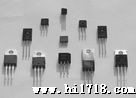
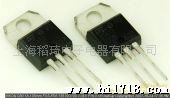
特优供应TOS东芝MOS管TK10A50D
价格:电议
地区:上海
电 话:86 021 37831020
传 真:86 021 37831462
图文详情
产品属性
相关推荐
TOSHIBA Field Effect Transistor Silicon N Channel MOS Type (π-MOSⅦ)
TK10A50D
Switching Regulator Applications
• Low drain-source ON-resistance: RDS (ON) = 0.62 Ω (typ.)
• High forward transfer admittance: ?Yfs? = 5.0 S (typ.)
• Low leakage current: IDSS = 10 μA (max) (VDS = 500 V)
• Enhancement mode: Vth = 2.0 to 4.0 V (VDS = 10 V, ID = 1 mA)
Absolute Maximum Ratings (Ta = 25°C)
Characteristics Symbol Rating Unit
Drain-source voltage VDSS 500 V
Gate-source voltage VGSS ±30 V
DC (Note 1) ID 10
Drain current Pulse (t = 1 ms)
(Note 1) IDP 40
A
Drain power dissipation (Tc = 25°C) PD 45 W
Single pulse avalanche energy
(Note 2) EAS 264 mJ
Avalanche current IAR 10 A
Repetitive avalanche energy (Note 3) EAR 4.5 mJ
Channel temperature Tch 150 °C
Storage temperature range Tstg −55 to 150 °C
Note: Using continuously under heavy loads (e.g. the application of high temperature/current/voltage and the
significant change in temperature, etc.) may cause this product to decrease in the reliability significantly even
if the operating conditions (i.e. operating temperature/current/voltage, etc.) are within the absolute maximum
ratings. Please design the appropriate reliability upon reviewing the Toshiba Semiconductor Reliability
Handbook (“Handling Precautions”/“Derating Concept and Methods’’) and individual reliability data (i.e.
reliability test report and estimated failure rate, etc).
Thermal Characteristics
Characteristics Symbol Max Unit
Thermal resistance, channel to case Rth (ch-c) 2.78 °C/W
Thermal resistance, channel to ambient Rth (ch-a) 62.5 °C/W
Note 1: Ensure that the channel temperature does not exceed 150°C.
Note 2: VDD = 90 V, Tch = 25°C (initial), L = 4.49 mH, RG = 25 Ω, IAR = 10 A
Note 3: Repetitive rating: pulse width limited by maximum channel temperature
This transistor is an electrostatic-sensitive device. Handle with care.
Unit: mm
JEDEC ?
JEITA SC-67
TOSHIBA 2-10U1B
Weight: 1.7 g (typ.)
1
3
2
1: Gate
2: Drain
3: Source
Internal