
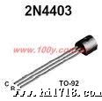

现货供应 开关三管2N4403
价格:电议
地区:广东 东莞市
电 话:86 0769 83033107
传 真:86 0769 83124718
图文详情
产品属性
相关推荐

特价现货供应 开关三极管2N4403
2N4403
Preferred Device
General Purpose
Transistors
PNP Silicon
Features
• Pb−Free Packages are Available*
MAXIMUM RATINGS
Rating Symbol Value Unit
Collector − Emitter Voltage VCEO 40 Vdc
Collector − Base Voltage VCBO 40 Vdc
Emitter − Base Voltage VEBO 5.0 Vdc
Collector Current − Continuous IC 600 mAdc
Total Device Dissipation
@ TA = 25°C
Derate above 25°C
PD
625
5.0
mW
mW/°C
Total Device Dissipation
@ TC = 25°C
Derate above 25°C
PD
1.5
12
W
mW/°C
Operating and Storage Junction
Temperature Range
TJ, Tstg −55 to
+150
°C
THERMAL CHARACTERISTICS
Characteristic Symbol Max Unit
Thermal Resistance, Junction−to−Ambient R JA 200 °C/W
Thermal Resistance, Junction−to−Case R JC 83.3 °C/W
Maximum ratings are those values beyond which device damage can occur.
Maximum ratings applied to the device are individual stress limit values (not normal
operating conditions) and are not valid simultaneously. If these limits are exceeded,
device functional operation is not implied, damage may occur and reliability may
be affected.
*For additional information on our Pb−Free strategy and soldering details, please
download the ON Semiconductor Soldering and Mounting Techniques Reference
Manual, SOLDERRM/D.
TO−92
CASE 29
STYLE 1
3
2
1
MARKING DIAGRAM
2N
4403
AYWW
See detailed ordering and shipping information in the package
dimensions section on page 3 of this data sheet.
ORDERING INFORMATION
https://onsemi.com
COLLECTOR
3
2
BASE
1
EMITTER
Preferred devices are recommended choices for future
use and best overall value.
2N4403 = Device Code
A = Assembly Location
Y = Year
WW = Work Week
= Pb−Free Package
(Note: Microdot may be in either location)
2N4403
http:/