A3212EUA 直插 a3212 双霍尔效应开关 国产替代 质量
价格:电议
地区:广东 深圳市
电 话:86 0755 33061996
传 真:86 0755 82501836
图文详情
产品属性
相关推荐
The A3211 and A3212 integrated circuits are ultrasensitive, pole independent Hall-effect switches with latched digital output. These devices are especially suited for operation in battery-operated, hand-held equipment such as cellular and cordless telephones, pagers, and palmtop computers. A 2.5 to 3.5 V operation and a unique clocking scheme reduce the average operating power requirements to less than 15 µW with a 2.75 V supply.
Unlike other Hall-effect switches, either a northorsouth pole of sufficient strength will turn the output on in the A3212, and in the absence of a magnetic field, the output is off. The A3211 provides an inverted output. The polarity independence and minimal power requirements allow these devices to easily replace reed switches for superior reliability and ease of manufacturing, while eliminating the requirement for signal conditioning.
Improved stability is made possible through chopper stabilization (dynamic offset cancellation), which reduces the residual offset voltage normally caused by device overmolding, temperature dependencies, and thermal stress.
This device includes on a single silicon chip a Hall-voltage generator, small-signal amplifier, chopper stabilization, a latch, and a MOSFET output. Advanced CMOS processing is used to take advantage of low-voltage and low-power requirements, component matching, very low input-offset errors, and small component geometries.
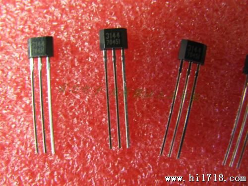
Four package styles provide magnetically optimized solutions for most applications. Miniature low-profile surface-mount package types EH and EL (0.75 and 0.50 mm nominal height) are leadless, LH is a 3-pin low-profile SMD, and UA is a three-pin SIP for through-hole mounting. Packages are lead (Pb) free (suffix, –T) with 100% matte tin plated leadframes.
完整型号:
| A3212EEHLT-T | 6-lead MLP |
A3212EEHLT-T 封装:6-lead MLP
A3212EELLT-T 封装:3-lead MLP
A3212ELHLT-T 封装:3-lead SOT
A3212EUA-T 封装:3-pin SIP