-
图文详情
-
产品属性
-
相关推荐
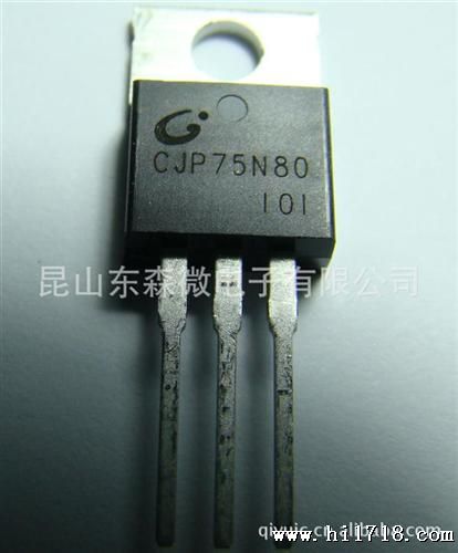
长电代理热销TO-220MOS管CJP75N80MOS类型NmosBVDSS 75VId(A) 80A,原厂代理,假一赔十。
75N80 N-Channel Power MOSFET
General Description
The CJ75N80 uses advanced trench technology and design to
Provide excellent RDS(on) with low gate charge. Good stability and
uniformity with high EAS .This device is suitable for use in PWM,
load switching and general purpose applications.
FEATURE
z Advanced trench process technology
z Special designed for convertors and power controls
z High density cell design for ultra low RDS(on)
z Fully characterized avalanche voltage and current
z Fast switching
z Avalanche energy 100% test
APPLICATIONS
z Power switching application
z Hard switched and high frequency circuits
z Uninterruptible power supply
Equivalent Circuit
Maximum ratings (at TA=25℃ unless otherwise noted)
Parameter Symbol Value Unit
Drain-Source voltage VDSS 75
Gate-Source Voltage VGS ±258
V
Drain Current(DC) at TC=25℃ 80
Drain Current(DC) at TC=100℃
ID(DC)
78
Drain Current-Continuous @Current-Pulsed(note1) IDM(pulse) 320
A
Peak diode recovery voltage dv/dt 0.6 V/ns
Power Dissipation PD 2 W
Derating factor 1.13 W/℃
Single Pulsed Avalanche Energy(note2) EAS 580 mJ
Thermal Resistance, Junction-to-Ambient 63
Thermal Resistance, Junction-to-Case 0.88
℃/W
Operating Junction and storage Temperature Range Tj, Tstg -55 ~175 ℃
Notes 1. Repetitive Rating: Pulse width limited by maximum junction temperature
2. EAS condition: Tj=25℃ , VDD=50V,VG=10V,L=0.3mH,ID=62A
TO-220
1. GATE
2. SOURCE
3. DRAIN
1 2 3
Electrical characteristics (at TA=25℃ unless otherwise noted)
Parameter Symbol Test Condition Min Typ Max Units
On/Off States
Drain-Source Breakdown Voltage BVDSS VGS = 0V, ID =250μA 75
Gate-Threshold Voltage VGS(th) VDS =VGS, ID =250μA 2.0 2.85 4.0
V
Gate-Body Leakage Current IGSS VDS =0V, VGS =±20V ±100 nA
Zero Gate Voltage Drain Current(TC=25℃) 1
Zero Gate Voltage Drain Current(TC=125℃)
IDSS VDS =75V, VGS =0V
10
μA
Drain-Source On-State Resistance RDS(on) VGS =10V, ID =40A 6.5 8.0 mΩ
Dynamic characteristics
Forward Transconductance gFS VDS =5V, ID =30A 60 S
Input Capacitance Ciss 3100
Output Capacitance Coss 310
Reverse Transfer Capacitance Crss
VDS =25V,VGS =0V,f =1MHz
260
pF
Total Gate Charge Qg 100
Gate-Source Charge Qgs 18
Gate-Drain Charge Qgd
VDS =30V,VGS =10V,ID =30A
27
nC
Switching times
Turn-On Delay Time td(on) 18.2
Rise Time tr 15.6
Turn-Off Delay Time td(off) 70.5
Fall Time tf
VDD=30V,
RL=15Ω, ID=2A,
VGS=10V,RG=2.5Ω
13.8
ns
Source-Drain Diode characteristics
Source-Drain Current(Body Diode) ISD 80
Pulsed Source-Drain Current(Body Diode) ISDM 320
A
Forward on Voltage VSD VGS =0V, ISD=40A, Tj=25℃ 1.2 V
Reverse Recovery Time(note1) trr 53
Reverse Recovery Charge (note1) Qrr
IF=75A, Tj=25℃,di/dt=100A/us
105
nS
Forward Turn-on Time t(on) Intrinsic turn-on time is negligible(turn-on dominated by LS+LD)
Notes1. Pulse Test : Pulse Width≤300μs, duty cycle ≤1.5%,RG=2.5Ω,Starting Tj=25℃


