


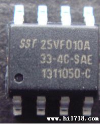
优势代理SST25VF010A-33-4C-SAE
价格:电议
地区:广东 深圳市
传 真:86 0755 33235359
图文详情
产品属性
相关推荐
Features
? 2.5V to 5.5V Input Supply Range
? 1.2MHz Current-Mode Boost Regulator
? Fast Transient Response to Pulse Load
? ±1% Accurate Output Voltage
? Built-In 20V/1.8A, 0.7Ω N-Channel MOSFET
? High Efficiency up to 90%
? Over-Current Protection
? Output Under-Voltage Protection
? High-Performance Operational Amplifier
? ±150mA Output Short-Circuit Current
? 12V/μs Slew Rate
? 12MHz, -3dB Bandwidth
? Rail-to-Rail Input and Output
? 600kHz Negative Charge Pump Driver for VGL
? 600kHz Positive Charge Pump Driver for VGH
? Power-On Sequence Control
? Thermal-Overload Protection
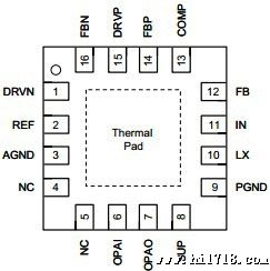
? TQFN3X3-16 Package
Applications
? Photo Frame
? GPS
? UMPC
General Description
The G5520 includes a high-performance boost regulator, a VCOMbuffer (unity gain OPA), a VGHcharge
pump driver, and a VGL charge pump driver for active-matrix thin-film transistor (TFT) liquid-crystal displays (LCDs).
The boost converter provides the regulated supply
voltage for the panel source driver ICs. The converter
is a high switching frequency (1.2MHz) current mode
regulator with an integrated 20V N-Channel 0.7Ω
MOSFET that allows the use of ultra-small inductors
and ceramic capacitors. It provides fast transient response to pulsed loading while achieving efficiency
over 90%. The device can produce output voltage as
high as 18V from an input as low as 2.8V.
The VCOMbuffer can drive the LCD VCOMvoltage that
features high short-circuit current (150mA), fast slew
rate (12V/μs), wide bandwidth (12MHz) and rail-to-rail
input/output.
A positive and a negative charge-pump driver provide
adjustable regulated output voltages VGHand VGLto
bias the TFT. Both the charge-pump driver operate
with 600kHz switching frequency.
The G5520 includes internal power-up sequencing,
over/under voltage protections of the boost converter,
and over temperature protection to ensure in safe operating.
The G5520 are available in a 16-pin 3X3TQFN packages