

3G模块
价格:电议
地区:广东 深圳市
手 机:13590199679
传 真:86 755 83281444
图文详情
产品属性
相关推荐
V100R001
Product Specification
Issue 1 (2009-01-20) Commercial in Confidence Page 7 of 60
1 Overview
1.1 Introduction
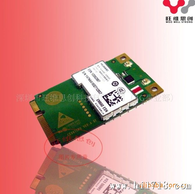
HUAWEI EM660 EVDO PC Embedded Module (hereinafter referred to as the EM660)
is aWirelessWide Area Network (WWAN) PC module based on the CDMA2000 1x,
the CDMA2000 1xEV-DO Rev. 0, and the CDMA2000 1xEV-DO Rev. A protocols. It is
a multi-mode wireless terminal for business professionals. In addition to messaging
services, the EM660 provides high-rate packet data services, supporting wireless
downloading at a speed as high as 3.1 Mbps and uploading at speed as high as 1.8
Mbps.
The EM660 supports the following standards:
l CDMA2000 1x
l CDMA2000 EV-DO Rev 0(EV-DOr0)
l CDMA2000 EV-DO Rev A(EV-DOrA)
The EM660 provides the following services:
l CDMA2000 1x packet data service
l EV-DOr0 packet data service
l EV-DorA packet data service
l CDMA2000 1x short message service (SMS)
l EV-DOr0 short message service (SMS)
l EV-DorA short message service (SMS)
l CDMA2000 1x PC voice
l EV-DOr0 PC voice
l EV-DorA PC voice
The EM660 can be connected to a PC via the Mini PCI Express interface. In the
service area of the CDMA2000 1x, EV-DOr0 or EV-DorA network, you can surf the
Internet, send messages and emails, telephone, and receive messages/emails
cordlessly. The EM660 is fast, reliable, and easy to operate. Thus, mobile users can
experience many new features and services with the EM660. These features and
services will enable a large number of users to use the EM660 and the average
revenue per user (ARPU) of operators will increase substantially.
PDF 文件使用 "pdfFactory Pro" 试用版本创建www.fineprint.com.cn
V100R001
Product Specification
Issue 1 (2009-01-20) Commercial in Confidence Page 8 of 60
Figure 1-1 shows the profile of the EM660.
Figure 1-1 Profile of the EM660
1.2 Key Features
The functional features of the EM660 are as follows:
l Supporting 800 MHz/1900 MHz frequency band
l Supporting the CDMA2000 1x standard
l Supporting the CDMA2000 1xEV-DO Rev. 0 standard
l Supporting the CDMA2000 1xEV-DO Rev. A standard
l Supporting receiving diversity
l Supporting R-UIM/ROM-UIM outside
l Supporting messaging
l Supporting high-rate packet data services
l Supporting PC Voice(Optional)
PDF 文件使用 "pdfFactory Pro" 试用版本创建www.fineprint.com.cn
V100R001
Product Specification
Issue 1 (2009-01-20) Commercial in Confidence Page 9 of 60
Table 1-1 lists the key features of the EM660.
Table 1-1 Key features of the EM660
Item Description
Standard l CDMA2000 1x RTT
l CDMA2000 1xEV-DO Rel. 0
l CDMA2000 1xEV-DO Rev. A
Data speed l Uplink: up tp 1.8 Mbit/s
l Downlink: up to 3.1 Mbit/s
CDMA 800 MHz Uplink: 824–849 MHz
Downlink: 869–894 MHz
Uplink: 1850–1910 MHz
Working
frequency
CDMA 1900 MHz
Downlink: 1930–1990 MHz
CDMA2000 1x RTT compliant with 3GPP2 CS0011-C: excelled -
104 dBm
Receiving
sensitivity
CDMA2000 1x EV-DO compliant with 3GPP2 CS0033-A: excelled -
105.5 dBm
Interfaces Mini PCI Express 1.2 interface (USB 2.0
Full Speed)
Support OS Windows 2000/Windows XP/Windows
Vista/Linux 2.6.18 or later versions
Maximum CDMA 800 MHz +23 dBm(Power Class 3)
transmit power
CDMA 1900 MHz +23 dBm(Power Class 2)
Maximum power consumption <3.3W
Working voltage 3.0~3.6V
Dimensions (L %W % H) 56.0mm×30.0mm×5.0mm
Weight About 8 g
Ambient Operating -10℃ to +55℃
temperature
Storage -40℃ to +85℃
Relative humidity 5%–95%
PDF 文件使用 "pdfFactory Pro" 试用版本创建www.fineprint.com.cn
V100R001
Product Specification
Issue 1 (2009-01-20) Commercial in Confidence Page 10 of 60
1.3 Hardware Overview
The hardware of the EM660 consists of three sections: baseband section, power
management (PM) section, and radio frequency (RF) section. External interfaces
include the antenna interface and the Mini PCI Express interface.
1.3.1 Hardware Logic Block Diagram
The EM660 is completed on a single-board. Figure 1-2 shows the hardware
functional block diagram.
Figure 1-2 Hardware functional block diagram
The circuitry of the EM660 consists of three sections: baseband section, RF section,
and PM section.
l The baseband section includes the baseband processor and DDR SDRAM/flash
MCP. It implements baseband signals processing, wireless protocols, and
management of various peripheral devices.
l The RF section includes the RF transceiver, PA, antenna switches, duplexer,
and antenna interfaces, and it supports receive diversity.
PDF 文件使用 "pdfFactory Pro" 试用版本创建www.fineprint.com.cn
V100R001
Product Specification
Issue 1 (2009-01-20) Commercial in Confidence Page 11 of 60
l The PMU section includes PM Part and DC-DC circuits, providing the power
supply and power management for the whole module.
1.3.2 External Hardware Interfaces
1. Antenna interface
The EM660 has a main antenna connector and an auxiliary antenna connector.
Mini PCI Express Interface
Screw holes
Auxiliary antenna
Main antenna
2. Mini PCI Express interface
The interface of the EM660 is a standard Mini PCI Express interface. The EM660
consists of several major signals, as shown in the following figure.
PDF 文件使用 "pdfFactory Pro" 试用版本创建www.fineprint.com.cn
V100R001
Product Specification
Issue 1 (2009-01-20) Commercial in Confidence Page 12 of 60
Figure 1-3 Mini PCI Express identification
− RUIM interface: The RUIM interface provides the interface for a RUIM card.
The RUIM card can be inserted into the PC.
− USB interface: This module can operate at USB low-speed (1.5 Mbits/sec)
and USB full-speed (12 Mbits/sec). It is compliant with USB 2.0
Specification,and available fromwww.usb.org.
− Because there is not a separate USB-controlled voltage bus, USB functions
implemented on EM660 which are expected to report as self-powered
devices.
− Auxiliary signals: The auxiliary signals provide some other functions.
− Power sources and grounds: The PCI Express Mini Card provides two power
sources, including the one at +3.3 Vaux (3.3Vaux) and the one at 1.5 V(+1.5
V). The EM660 uses the +3.3 voltage as the power supply.
PDF 文件使用 "pdfFactory Pro" 试用版本创建ÿwww.fineprint.com.cn
V100R001
Product Specification
Issue 1 (2009-01-20) Commercial in Confidence Page 13 of 60
1.4 Software Overview
Figure 1-4 Software logic block diagram
Descriptions of the functional modules in the system architecture are as follows.
Firmware Drivers
The firmware drivers include drivers of the RF module, flash, and all the peripherals
such as the UIM card and USB device.
Platform Service Subsystem
The platform service subsystem initializes programs, diagnoses, downloads data,
and serves as a watchdog.
Application Service Subsystem
The application service subsystem consists of various application services and a
CDMA 1X/EVDO dual mode protocol stack. Application services handle the
commands and data sent from PC side according to service categories, and deliver
them to the protocol stack. The protocol stack communicates with the network side to
Dashboard
PC Drivers
Application Service
Subsystem
Firmware Drivers
Platform Service Subsystem
PC
Firmware
Mini PCIE interface
Firmware
PC Drivers
Dashboard
PDF 文件使用 "pdfFactory Pro" 试用版本创建Àwww.fineprint.com.cn
V100R001
Product Specification
Issue 1 (2009-01-20) Commercial in Confidence Page 14 of 60
process the commands and data, and returns response from network to application
services. Finally, application services return responses to PC side.
The main application services are as follows:
l Call management service
l SMS service
l 1X/EVDO data service
PC Drivers
The PC drivers are used to implement functions such as the interaction between the
dashboard and the firmware.
Dashboard
The dashboard enables the PC side to display the interfaces of initiating or
answering a call, and sending and receiving messages. It provides the interface for
1X/EVDO network accessing and periodically refreshes the interface of the current
USB modem status. The interface is provided to the end users.
PDF 文件使用 "pdfFactory Pro" 试用版本创建www.fineprint.com.cn
V100R001
Product Specification
Issue 1 (2009-01-20) Commercial in Confidence Page 15 of 60
2 Mechanical Specifications
2.1 Dimensions and interfaces
2.1.1 Dimensions and interfaces of the EM660
The dimensions of the EM660 are 51 mm (length) × 30 mm (width) × 5 mm (height),
which comply with the standard dimensions specified in the PCI Express Mini Card
Electromechanical Specification Revision 1.2. Figure 2-1 shows the dimensions of
the EM660 in details.
Figure 2-1 Dimensions of the EM660
Figure 2-2 shows the appearance of the interfaces on the EM660.
PDF 文件使用 "pdfFactory Pro" 试用版本创建www.fineprint.com.cn
V100R001
Product Specification
Issue 1 (2009-01-20) Commercial in Confidence Page 16 of 60
Figure 2-2 Appearance of the interfaces on the EM660
data signal.
Input/Output
11 REFCLK- NC Not connected. –
12 UIM_CLK UIM_CLK External UIM/UIM
clock signal.
Output
13 REFCLK+ NC Not connected. –
PDF 文件使用 "pdfFactory Pro" 试用版本创建www.fineprint.com.cn
V100R001
Product Specification
Issue 1 (2009-01-20) Commercial in Confidence Page 21 of 60
Definition of the EM660Mini PCI Express pins
Pin
No.
Mini PCI
Express
Standard
Description
HUAWEI Pin
Description
Additional
Description
Direction to
Module
14 UIM_RESET UIM_RESET External UIM/UIM
reset signal.
Output
15 GND GND Mini Card ground. –
16 UIM_Vpp NC Not connected. –
17 Reserved NC Not connected. –
18 GND GND Mini Card ground. –
19 Reserved NC Not connected. –
20 W_DISABLE# W_DISABLE_N For ending the
wireless
communications
Input
21 GND GND Mini Card ground. –
22 PERST# PERST# For forcing a
hardware reset on
the card.
Input
23 PERn0 NC Not connected. –
24 3.3Vaux NC Not connected. –
25 PERp0 NC Not connected. –
26 GND GND Mini Card ground. –
27 GND GND Mini Card ground. –
28 1.5 V NC Not connected. –
29 GND GND Mini Card ground. –
30 SMB_CLK NC Not connected. –
31 PETn0 NC Not connected. –
32 SMB_DATA NC Not connected. –
33 PETp0 NC Not connected. –
34 GND GND Mini Card ground. –
35 GND GND Mini Card ground. –
36 USB_D- USB_D- USB signal D-. Input/Output
37 GND GND GND –
38 USB_D+ USB_D+ USB signal D+. Input/Output
PDF 文件使用 "pdfFactory Pro" 试用版本创建www.fineprint.com.cn
V100R001
Product Specification
Issue 1 (2009-01-20) Commercial in Confidence Page 22 of 60
Definition of the EM660Mini PCI Express pins
Pin
No.
Mini PCI
Express
Standard
Description
HUAWEI Pin
Description
Additional
Description
Direction to
Module
39 3.3Vaux VCC_3V3 3.3V DC supply
rail from the PC
side.
Input
40 CPUSB# GND GND –
41 3.3Vaux VCC_3V3 3.3V DC supply
rail from the PC
side.
Input
42 LED_WWAN# LED_WWAN Active-low LED
signal for
indicating the state
of the card.
Output
43 GND GND GND –
44 LED_WLAN# NC Not connected. –
45 Reserved PCM_CLK PCM clock Output
46 LED_WPAN# NC Not connected. –
47 Reserved PCM_DOUT PCM data output Output
48 1.5 V NC Not connected –
49 Reserved PCM_DIN PCM_data input Input
50 GND GND Mini Card Ground –
51 Reserved PCM_SYNC PCM frame
synchronization
Output
52 3.3Vaux VCC_3V3 3.3V DC supply
rail from the PC
side.
Input
PDF 文件使用 "pdfFactory Pro" 试用版本创建www.fineprint.com.cn
V100R001
Product Specification
Issue 1 (2009-01-20) Commercial in Confidence Page 23 of 60
3.2 Pin Descriptions
3.2.1 Digital Signal DC Characteristics
Table 3-2 Digital signal DC characteristics
Symbol Description Minimum Maximum Unit Notes
VIH High-level input voltage,
CMOS/Schmitt
0.65*
VDD_PX
VDD_PX
+0.3
V 1
VIL Low-level input voltage,
CMOS/Schmitt
–0.3 0.35-
VDD_PX
V 1
VOH High-level output voltage,
CMOS
VDD_PX-
0.45
VDD_PX V 1
VOL Low-level output voltage,
CMOS
0 0.45 V 1
IIH Input high leakage current – 1 μA 1
IIL Input low leakage current –1 – μA 1
IIHPD Input high leakage current
with pull-down
3 30 μA 1
IILPU Input low leakage current
with pull-up
–30 –3 μA 1
IOZH High-level, three-state
leakage current
– 1 μA 1
IOZL Low-level, three-state
leakage current
–1 – μA 1
IOZHPD High-level, three-state
leakage current with pulldown
3 30 μA 1
IOZLPU Low-level, three-state
leakage current with pullup
–30 –3 μA 1
CIN Input capacitance – 7 pF 1, 2
Notes:
1. Table 3-2 lists the universal specifications of the signals. Any difference from the universal
specifications is listed in the related chapter or section.
2. The input capacitance value is guaranteed by design and not completely tested.
PDF 文件使用 "pdfFactory Pro" 试用版本创建www.fineprint.com.cn
V100R001
Product Specification
Issue 1 (2009-01-20) Commercial in Confidence Page 24 of 60
3.2.2 Power Sources and Grounds
The PCI Express Mini Card provides two power sources: one is +3.3Vaux (3.3 Vaux)
and the other is 1.5V (+ 1.5 V). For the EM660, +3.3Vaux is the only supply voltage
available. The input voltage is +3.3 V ± 9%, as specified by PCI Express Mini CEM
Specifications 1.2.
Table 3-3 Power and ground specifications
Name Pins Minimum Type Maximum
VCC 2, 39, 41, and 52 3.0 V 3.3 V 3.6 V
GND 4, 9, 15, 18, 21, 26, 27, 34, 35,
37, 43, and 50
0 V
3.2.3 USB Signals
The EM660 is compliant with USB 2.0 specification. It supports full-speed and lowspeed.
Table 3-4 USB pins
Name Pin Description Direction to Module
USB D- 36 USB data signal D- Input/Output
USB D+ 38 USB data signal D+ Input/Output
The USB interface is powered directly from the 3.3 V supply. The USB input/output
lines are compatible with the USB 2.0 3.3 V signal specifications.
Table 3-5 USB signal DC characteristics
VOHmin VOLmax VIHmin VILmax
2.8V 0.3V 2V 0.8V
3.2.4 RUIM Signals
The RUIM is a smart card for CDMA cellular applications; it provides personal
authentication information that allows the mobile station or handset to be connected
with the network. The RUIM card can be inserted into any CDMA RUIM equipped
handset to enable its user to receive or make calls and receive other subscribed
services.
The internal power management circuits, UIM circuity, and UIM pads allow for
implementing both 1.8 V and/or 2.85 V cards via a direct connection.
PDF 文件使用 "pdfFactory Pro" 试用版本创建www.fineprint.com.cn
V100R001
Product Specification
Issue 1 (2009-01-20) Commercial in Confidence Page 25 of 60
Key RUIM features are:
l Shared interface for RUIM applications, thereby further supporting CDMA
networks
l Selectable clock source
l Supports dual voltage cards (2.85 V and 1.8 V)
PDF 文件使用 "pdfFactory Pro" 试用版本创建www.fineprint.com.cn
V100R001
Product Specification
Issue 1 (2009-01-20) Commercial in Confidence Page 26 of 60
Table 3-6 RUIM pins
Pin Name Description Direction to
Module
8 UIM_PWR Power source for the external
UIM/UIM.
Output
10 UIM_DATA External UIM/UIM data signal. Input/Output
12 UIM_CLK External UIM/UIM clock signal. Output
14 UIM_RESET External UIM/UIM reset signal. Output
16 UIM_Vpp Programming power connection used
to program EEPROM of first
generation ICCs, but not used now.
Not connected
Notes:
It is recommended that the UIM card is inserted only after the power of the module is
disconnected, otherwise the UIM card can be destroyed.
RUIM interface schematic reference:
There is no UIM card interface circuit in the EM660 module, and users need to add
the RUIM interface circuit. The definition of interface signals and the typical RUIM
interface schematic are as follows.
Figure 3-1 RUIM interface schematic on user’s PC
PDF 文件使用 "pdfFactory Pro" 试用版本创建www.fineprint.com.cn
V100R001
Product Specification
Issue 1 (2009-01-20) Commercial in Confidence Page 27 of 60
Design guide
The RUIM signals are connected to the Mini PCI Express card connector (the card
edge connector) and pass through an EMI filtering and ESD protection circuit on the
module board before entering the EM660 processor. There is also an EMI filtering
and ESD protection circuit between UIM card interface and Mini PCI interface on the
user’s board.
1. Power supply
The UIM interface is powered by an LDO regulator. The default value of this regulator
is 2.85 V. The power of the regulator is programmable in the range of 1.5 V to 3.05 V
and is expected to be set to 2.85 V or 1.8 V.
2. Modem signals
After a power-on or reset, the RUIM signals are activated to detect if a UIM card is
present and to initialize it if it exists. Once a card has been detected and initialized,
the interface is always on. However, the clock signal is only activated when data is
actually being transferred. The RUIM signals from the MSM are connected to the
level translators and then to the Mini Card host connector.
These levels exceed those required in ISO/IEC 7816-3.
3. ESD protection
Since the UIM is a CMOS device, ESD protection devices should be placed near to
the UIM connector to provide protection. In addition, all the UIM interface signals
should be bypassed with a 33 pF capacitor.
4. Routing recommendations
The UIM interface signals consist of four signals that are Vcc, RST, CLK, and IO (Vpp
is also connected but not used in many applications). Due to the relatively low clock
frequencies involved, the concern is not the degradation of the UIM signals
themselves. The main concern is routing of the UIM interface signals through areas
considered to be of high risk for RF noise coupling (crosstalk and RF contamination)
which can desensitize the radio circuitry. The general guidelines that should be
followed are listed as follows:
l It is recommended that these signals should be routed over a contiguous ground
plane.
l UIM interface signals should not be routed near high transient signals (power
supply chokes and DC/DC switching FETs).
l Avoid routing of these signals near output connectors.
l Keep UIM interface signals isolated from other signals. 2x width spacing (1.5x
min) between UIM interface signals and all other signal routing is recommended.
PDF 文件使用 "pdfFactory Pro" 试用版本创建www.fineprint.com.cn
V100R001
Product Specification
Issue 1 (2009-01-20) Commercial in Confidence Page 28 of 60
3.2.5W_DISABLE# Signal
The W_DISABLE# signal is provided to allow users to disable wireless
communications add-in cards. When theW_DISABLE# signal is asserted, all radios
should be disabled.When the W_DISABLE# signal is not asserted, the radio may
transmit if not disabled by other means such as software.
The W_DISABLE# signal is an active low signal with internal 100 kΩ pull-up resistor
that shall disable radio operation when being asserted (driven low) by the system.
Due to the potential of a software disable state, the combination of the software state
andW_DISABLE# assertion state must be determined before the normal operation is
resumed. Table 3-8 lists this requirement on the function of W_DISABLE# and the
software control setting. For example, the radio RF operation remains disabled
unless both the hardware and software are set to enable the RF features of the card.
Table 3-7 W_DISABLE_N signal
Pins Name Description Direction to Module
20 W_DISABLE_N Close wireless communications Input
Table 3-8 Radio operational states
W_DISABLE# SW Control Setting* Radio Operation
High Enabled Enabled
High Disabled
Low Enabled
Low Disabled
Disabled
* This control setting is implementation specific; this column represents the collective
intention of the host software to manage radio operation.
If PC uses a hardware switch or EC(Embedded Controller) control W_DISABLE#,
3.3V VCC Main Voltage and W_DISABLE# must meet Figure 3-2 power sequences.
Figure 3-2 power sequences timing diagram
Notes:
We strongly recommend controlling this pin via hot-keys or a hardware switch. There are three
points as bellow:
PDF 文件使用 "pdfFactory Pro" 试用版本创建www.fineprint.com.cn
V100R001
Product Specification
Issue 1 (2009-01-20) Commercial in Confidence Page 29 of 60
1. If we don’t turn off radio manually, radio will be on when module is powered on.
2. End users need turn off radio at some situation like on an airplane.
3. According to Mini-PCIE specification, we must turn off radio through hardware or software.
Nearly all PC companies obey this specification.
3.2.6 LED_WWAN# Signal
The LED_WWAN signal of the EM660 can tolerate up to the voltage of 5 V and
absorb the current up to150 mA. According to the given circuit, in order to reduce the
current of the LED, a resistance of 1 kΩ must be placed in series with the LED.
Table 3-9 LED_WWAN signal
Pins Name Description Additional
Description
Direction to
Module
42 LED_WWAN Active-low LED signal
for indicating the status
of the module.
L: Light on
H: Light off
Output
This signal is used to display the state of WWAN. The reference circuit diagram is
shown in the following figure.
Figure 3-3 LED_WWAN# signal reference circuit diagram
Notes:
The wink mode of the LED can be customized by the demand of the client.
3.2.7 PERST# Signal
The PERST# signal has an internal pull-up. The active low input is used to hard reset
the module.
100 n
1 kΩ LED
Module
VCC
LED_WWAN signal
1 kΩ
PC
PDF 文件使用 "pdfFactory Pro" 试用版本创建ÿwww.fineprint.com.cn
V100R001
Product Specification
Issue 1 (2009-01-20) Commercial in Confidence Page 30 of 60
The PERST# signal is de-asserted by the host to indicate that system power sources
are within the specified voltage tolerance and are stable. PERST# can be asserted
by the host when power is switched off and also can be used by the system to force a
hardware reset on the card. However, a hardware reset is not required during normal
operation and may only be used in case of module malfunction.
A hard reset of the module will result in a surprise removal of the module on the USB
controller and cause the operating system to unload the device drivers. This will lead
to a delay before the operating system discovers the device again. To avoid this delay,
the PERST# pin should not be used in normal operation or in standby mode.
Table 3-10 PERST# signal
Pins Name Description Additional
Description
Direction to
Module
22 PERST# Force a hardware reset
on the card.
H: normal or
standby.
L: Reset the
module.
Input
3.2.8 NC Pins
The NC pins are not internally connected in the EM660.
3.3 Power Supply and Consumption
3.3.1 Power Supply
The EM660 is supplied by 3.3 V power source, which must satisfy all requirements of
PCI Express Mini CEM specifications, such as voltage tolerance and peak and
normal current. The detailed requirements are listed in Table 3-11.
Table 3-11 Power requirements
Power Voltage Tolerance Peak (Maximum) Normal (Maximum)
3.3 V ±9% 2750 mA 1100 mA
Notes:
To minimize the RF radiation through the PCI-E interface, you can add a 33 pF ceramic capacitor
to ground on every pin of the PCI-E on the host side except USB D+/D-.
PDF 文件使用 "pdfFactory Pro" 试用版本创建www.fineprint.com.cn
V100R001
Product Specification
Issue 1 (2009-01-20) Commercial in Confidence Page 31 of 60
3.3.2 Power Consumption
The power consumptions of the EM660 in different scenarios are respectively listed
in Table 3-12, and Table 3-14.
Table 3-12 DC power consumption (CDMA)
Band Frequency
Channel
Test Value Units Power (dBm)
218 1dBm Tx Power
dBm Tx Power
577
mA
24dBm Tx Power
215 1dBm Tx Power
dBm Tx Power
580
mA
23.6dBm Tx Power
217 1dBm Tx Power
323 10dBm Tx Power
BAND1
(Cell 800M)
1013
648
mA
23.7dBm Tx Power
307 1dBm Tx Power
dBm Tx Power
623 23.9dBm Tx Power
303 1dBm Tx Power
dBm Tx Power
649 23.9dBm Tx Power
311 1dBm Tx Power
352 10dBm Tx Power
BAND2
(Pcs1900M)
1175
740 24dBm Tx Power
Table 3-13 DC power consumption (EVDO)
Band Frequency
Channel
Test Value Units Power (dBm)
299 1dBm Tx Power
dBm Tx Power
600
mA
24.3dBm Tx Power
304 1dBm Tx Power
BAND1
(Cell 800M)
777
331
mA
10dBm Tx Power
PDF 文件使用 "pdfFactory Pro" 试用版本创建www.fineprint.com.cn
V100R001
Product Specification
Issue 1 (2009-01-20) Commercial in Confidence Page 32 of 60
Band Frequency
Channel
Test Value Units Power (dBm)
627 24dBm Tx Power
300 1dBm Tx Power
dBm Tx Power
645
mA
23.9dBm Tx Power
320 1dBm Tx Power
dBm Tx Power
625 24.2dBm Tx Power
321 1dBm Tx Power
dBm Tx Power
680 24.3dBm Tx Power
323 1dBm Tx Power
357 10dBm Tx Power
BAND2
(Pcs1900M)
1175
750 24.3dBm Tx Power
Table 3-14 DC power consumption(Idle and Suspend)
Scenario Suspend
Offline Enabled Offline Disabled
Unit
CDMA2000 1X 2.80 4.10 mA
EVDO 2.80 4.58 mA
Notes:
The EM600 module has three different operating mode:
1:active mode;
2:suspend mode ;
3:power off mode.
PDF 文件使用 "pdfFactory Pro" 试用版本创建www.fineprint.com.cn
V100R001
Product Specification
Issue 1 (2009-01-20) Commercial in Confidence Page 33 of 60
4 RF Specifications
4.1 Operating Frequencies
Table 4-1 RF bands
EM660
Operating Band Tx Rx
CDMA Cellular 824–849 MHz 869–894 MHz
CDMA PCS 1850–1910 MHz 1930–1990 MHz
4.2 Conducted Rx sensitivity and Tx power
Table 4-2 EM660 conducted Rx sensitivity
Item 3GPP Protocol Claim Unit
CDMA Cellular <–104 dBm
CDMA PCS <–104 dBm
Table 4-3 EM660 conducted Tx power
Item 3GPP Protocol Claim Unit
CDMA Cellular >23 dBm
CDMA PCS >23 dBm
% = Bit Error Rate or Block Error Rate
PDF 文件使用 "pdfFactory Pro" 试用版本创建www.fineprint.com.cn
V100R001
Product Specification
Issue 1 (2009-01-20) Commercial in Confidence Page 34 of 60
4.3 Antenna Design Requirements
4.3.1 Recommended Index of the Module Antennas
Table 4-4 Recommended index of the main antenna
Working frequency 824–960 MHz and 1710–2170 MHz
Port impedance 50 Ohm
Port standing wave < 2.0
Peak gain > 0 dBi
Antenna efficiency > 60%
Polarization Linear polarization
Pattern Omnidirectional
GPS shares the auxiliary antenna with receiver diversity, when GPS session is
ongoing, the receiver diversity functionality will be turned off automatically and the
auxiliary antenna will serve for GPS. However, when GPS session is closed, the
antenna will be switched back to serve for receiver diversity.
Table 4-5 Recommended index of the auxiliary antenna
Working frequency 869–960 MHz, 1930–1990 MHz and 2110–2170 MHz
Port impedance 50 Ohm
Port standing wave < 2.0
Peak gain > –3 dBi
Antenna efficiency > 30%
Polarization Linear polarization
Pattern Omnidirectional
Table 4-6 Recommended index of the GPS antenna
Working frequency 1574.42MHz~1576.42 MHz
Port impedance 50 Ohm
Antenna efficiency > 50%
Polarization Circular polarization or Linear polarization
Pattern Omnidirectional
Table 4-7 Recommended index of the isolation between the main antenna and the
auxiliary antenna
Antenna isolation < –10 dB
PDF 文件使用 "pdfFactory Pro" 试用版本创建www.fineprint.com.cn
V100R001
Product Specification
Issue 1 (2009-01-20) Commercial in Confidence Page 35 of 60
Because the PC has other internal antennas such as theWLAN antenna, to ensure
the proper operation of each communication system, requirements on antenna
isolation between different communication systems should be considered. Table 4-8
lists the recommended index of the antenna isolation.
Table 4-8 Recommended index of the isolation between the module antennas and
other PC antennas
Antenna isolation < –20 dB
4.3.2 Design Recommendations
Recommendations for Designing the Module Antennas
The design recommendations are as follows:
1. It is recommended that the module antennas are designed at the upper edge,
left edge or right edge of the PC screen. Designing the antenna at the upper
edge is better.
2. When designing the main antenna and the auxiliary antenna, the requirement on
the antenna isolation should be considered (the recommended value is listed in
Table 4-7). Meanwhile, try to keep the distance between the main antenna and
the auxiliary antenna as large as possible for optimizing the space diversity. For
example, you can place the main antenna at the upper left corner of the PC
screen and place the auxiliary antenna at the upper right corner of the PC
screen.
3. You are recommended to design the antenna pattern as the horizontal polarized
omnidirectional pattern that facilitates the reception of strong signals especially
in outdoor environments.
4. Besides the module antennas, a PC has other internal antennas, such as the
WLAN antenna. Therefore, when designing the module antennas, the
requirement on the isolation between module antennas and other PC antennas
should be considered (the recommended value is listed in Table 4-8). Keep
proper distance between antennas if possible. To reduce the interference
between antennas, it is not recommended that an antenna is designed closely
next to another one.
5. Carefully design the metallic components (such as the external frame of the
metallic shell) in and near the antenna area with considering the effects on the
antenna performance (such as whether the frequency offset of the antenna
occurs and whether the antenna pattern is deformed).
Recommendations for Handling the Interference Sources
On a PC, there are various interference sources, such as the LCD, CPU, audio
circuits, and power supply. All the interference sources emit interference signals that
affect the normal operation of the module. For example, the module sensitivity can be
decreased due to interference signals. Therefore, during the design, you need to
consider how to lessen the effects of interference sources on the module. You can
PDF 文件使用 "pdfFactory Pro" 试用版本创建www.fineprint.com.cn
V100R001
Product Specification
Issue 1 (2009-01-20) Commercial in Confidence Page 36 of 60
take the following measures: Use an LCD with optimized performance; shield the
LCD interference signals; shield the signal cable of the PC; or design filter circuits.
4.4 Offline Mode
The offline mode can be enabled by the following method:
l Through hardware: The W_DISABLE pin can be used to control the RF circuit.
When the pin is driven to the high level, the RF circuit works; when the pin is
driven to the low level, the RF circuit does not work.
PDF 文件使用 "pdfFactory Pro" 试用版本创建www.fineprint.com.cn
V100R001
Product Specification
Issue 1 (2009-01-20) Commercial in Confidence Page 37 of 60
5 Software and Tools
Huawei can provide the firmware, PC driver, dashboard, and software. The firmware
runs on the module; the PC driver and dashboard run on the PC and communicate
with the firmware to realize all module functions. Huawei can also provide the
software for upgrading the firmware and debugging the problems.
5.1 Firmware
The firmware is software on the module. It accepts commands and data from the host
through USB. The host can send AT commands to enable the firmware to connect,
disconnect, or query.
5.1.1 Version Descriptions
In the version number, the front digits is the firmware version that can differ which
version is newer. The upper bits (except the last two bits) has boarder meaning in the
version name. If the customer has special order to our common version, the order will
be implemented in special version. The version is named by last two bits, but the
front bits are still the common version.
5.2 Drivers
A driver is a program running on the host system, which allows the host system to
interact with the Huawei wireless module. The driver communicates with the firmware
of the module by using the USB protocol.
The USB manufacturer ID for all Huawei USB devices is 0x12D1.
The USB product ID for the EM660 device is 0x1001. There are three USB interfaces
in the USB product ID.
XX.XXX.XX.XX.XX
Firmware version Customization version
PDF 文件使用 "pdfFactory Pro" 试用版本创建www.fineprint.com.cn
V100R001
Product Specification
Issue 1 (2009-01-20) Commercial in Confidence Page 38 of 60
5.2.1Windows Drivers
Huawei provides windows drivers to support Windows 2000/XP/Vista.
Huawei provides the following two ways to install the drivers:
l The drivers are packed in the dashboard, and they will be installed during the
dashboard installation.
l The drivers are provided as an installer, which can be directly installed under
Windows 2000/XP/Vista.
After the drivers are installed, when the EM660 is connected to the USB bus, it will be
detected as a USB device and start enumerating. During this process, multiple
drivers are loaded. These drivers expose a number of virtual COM ports.
InWindows OSs, you can check the enumerated devices and their configuration in
the device manager. If you switch to View by connection, the device manager
displays the main USB device and interfaces, as shown in Figure 5-1, this figure is
just a sample, different products maybe add or remove some ports.
Figure 5-1 HUAWEI USB device and interfaces
The following interfaces and ports are supported by EM660:
l HUAWEI Mobile Connect – 3G Modem: used to set up a data connection.
l HUAWEI Mobile Connect – 3G Application Interface: used to write and read
diagnostics data.
l HUAWEI Mobile Connect – 3G PC UI Interface: used to send AT commands and
read their responses.
5.2.2 Linux Drivers
The EM660 can be used in the Linux OS that the kernel version is 2.6.18 or later. If
the kernel is a standard one, it means that the kernel is not customized and the driver
PDF 文件使用 "pdfFactory Pro" 试用版本创建www.fineprint.com.cn
V100R001
Product Specification
Issue 1 (2009-01-20) Commercial in Confidence Page 39 of 60
is already packed in the kernel; if the kernel is customized and the driver has been
discarded, Huawei will provide the Linux driver for customers to merge the driver into
the kernel again.
5.3 Dashboard
5.3.1Windows Dashboard
Huawei can provide the dashboard to manage the connection and other functions
under Windows 2000/XP/Vista.
Figure 5-2 shows the screenshot of Huawei common dashboard.
Figure 5-2 Screenshot of Huawei common dashboard
Table 5-1 lists the dashboard specifications.
Table 5-1 Windows dashboard specifications
Item Description
Writing/Sending/Receiving
Sending/Receiving the SMS
SMS
Group sending
PDF 文件使用 "pdfFactory Pro" 试用版本创建www.fineprint.com.cn
V100R001
Product Specification
Issue 1 (2009-01-20) Commercial in Confidence Page 40 of 60
Item Description
New message prompt (visual prompt/audio prompt)
Current connection:
l Duration
l Send/Receive flow
l Send/Receive rate
Flow display
and statistics
(data services)
Traffic statistics: You can view the traffic information of the day,
the month, or the year.
Stores the contacts in the hard disk of the PC, the UIM card and
the device.
Messages can be sent through the phonebook.
Phonebook
Importing/Exporting: Import or export contacts between the UIM
card and a PC or a file of supported formats.
Network
connection
setup
l Profile management: create, delete, and edit.
l Set up the network connection.
Network status
display
Signal status, system mode, and so on.
network
connection
types
Selection of network connection types, for example:
l 1X only
l EVDO only
l Hybrid
PIN
management
Activating or deactivating PIN, PIN lock, changing PIN, and
unblocking PIN by using the PUK
System
requirement
l Windows 2000 SP4,Windows XP SP2, Windows Vista
l The hardware system on the PC should meet or exceed the
recommended system requirements for the installed version
of OS.
l Display resolution: 800 × 600 or above
Notes:
CPU = central processing unit
PIN = personal identification number
PUK = PIN unblocking key
5.3.2 Linux Dashboard
The Linux dashboard can be developed separately according to the customization
requirements of customers.
PDF 文件使用 "pdfFactory Pro" 试用版本创建www.fineprint.com.cn
V100R001
Product Specification
Issue 1 (2009-01-20) Commercial in Confidence Page 41 of 60
5.4 Tools
5.4.1 Firmware Update Tool
The Windows-based update tool provided by Huawei is used to update the firmware
of the EM660.
The following figures (from Figure 5-3 to Figure 5-9)show the procedure for using the
EM660 update tool.The EM660 update procedure is the same as EM660.
Figure 5-3 EM660 update tool
PDF 文件使用 "pdfFactory Pro" 试用版本创建www.fineprint.com.cn
V100R001
Product Specification
Issue 1 (2009-01-20) Commercial in Confidence Page 42 of 60
Figure 5-4 Screenshot of the EM660 update tool–Searching the device
Figure 5-5 Screenshot of the EM660 update tool–Detected devices
PDF 文件使用 "pdfFactory Pro" 试用版本创建www.fineprint.com.cn
V100R001
Product Specification
Issue 1 (2009-01-20) Commercial in Confidence Page 43 of 60
Figure 5-6 Screenshot of the EM660 update tool–Warning
Figure 5-7 Screenshot of the EM660 update tool–Downloading programs
PDF 文件使用 "pdfFactory Pro" 试用版本创建www.fineprint.com.cn
V100R001
Product Specification
Issue 1 (2009-01-20) Commercial in Confidence Page 44 of 60
Figure 5-8 Screenshot of the EM660 update tool–Update succeeded
Figure 5-9 Screenshot of the EM660 update tool–To finish the update
PDF 文件使用 "pdfFactory Pro" 试用版本创建www.fineprint.com.cn
V100R001
Product Specification
Issue 1 (2009-01-20) Commercial in Confidence Page 45 of 60
5.4.2 Engineering Tools
Qualcomm has an extensive debugging and tracing toolset available for their
chipsets. Huawei EM660 is compatible with these tools from Qualcomm, such as
QXDM, QPST, and QCAT.
5.4.3 Debugging Board
I. Functions and Usage of the Debugging board
The debugging board developed by Huawei is an auxiliary board that is used to
debug the EM660.When the debugging board is used, you can connect the module
to a PC through a USB cable.When the module works normally, the debugging
functions can be implemented. The debugging board provides multiple interfaces,
such as the USB port, DC power jack, mini PCI-E connector, BTB connector, UIM
card socket, RF connectors, PCM audio interface, and serial ports (including a 4-pin
serial port and a serial port that all pins are led out). The test points of key signals are
led out on the debugging board. In addition, the debugging board is designed with
switches or pins of commonly used signals such as the reset signal and the enable
signal, for converting the working state of the module.
The debugging board can be used to test the performance of the module. Both the
wired connection test (connect the module to the CMU200) and the wireless
connection test (connect the module to the antennas) can be implemented. The
signal points can also be tested when you maintain and repair the module.
II. Structure of the Debugging board
Figure 5-10 Structure of the debugging board
Notes:
1. RF connector: RF switch, bend, female.
2. RF connector: coaxial connector, straight, male.
3. RF connector: RF switch, straight, female.
4. Connector latch: It works with the mini PCI-E connector and is used for fixing the module.
PDF 文件使用 "pdfFactory Pro" 试用版本创建www.fineprint.com.cn
V100R001
Product Specification
Issue 1 (2009-01-20) Commercial in Confidence Page 46 of 60
5. Mini PCI-E connector: female, 52-pin, straight.
6. UIM card socket: It is used to holding the inserted UIM card.
7. USB connector and mini USB B-type receptacle: Side-plugging USB connector.
III. Method for Connecting the Debugging Board
1. Diagram of connecting the module to the CMU200
Figure 5-11 Diagram of connecting the module to the CMU200
Figure 5-11 shows the connection method that can be used to test the wired
connection comprehensively, software and key signal points.
2. Diagram of connecting the module and the antenna
Figure 5-12 Diagram of connecting the module and the antenna
Figure 5-12 shows the wireless connection method that can be used to simulate the
actual wireless environment for testing the software and key signal points.
Auxiliary
Main
PDF 文件使用 "pdfFactory Pro" 试用版本创建ÿwww.fineprint.com.cn
V100R001
Product Specification
Issue 1 (2009-01-20) Commercial in Confidence Page 47 of 60
IV. Installation of the Debugging board
l Connect the devices and set up the test environment according to Figure 5-11 or
Figure 5-12. Then properly connect one end of the module to the mini PCI-E
connector and fix the other end of the module by well locking the connector latch.
Insert the UIM card into the UIM card socket. Then connect the debugging board
to the PC through a USB cable. You can connect the USB cable only when the
module is properly connected to the mini PCI-E connector and fixed.
l When performing the wired connection test, connect the CMU200 to the RF
interface of the module by using the module-dedicated RF cable. (For the
connection method, see Figure 5-11.) The compensation for the line loss of the
CMU200 is about 0.7 dBm.
l When performing the wireless connection test, connect the module to the
debugging board by using the RF cable. Then connect the antennas to the RF
interface of the module directly. (For the connection method, see Figure 5-12.)
V. Test Method
After the preceding operations, if the LED below the mini PCI-E connector, you can
infer that the program is running. Then the following functions can be realized by
using the debugging board.
1. Controlling the states and testing the performance in each state
The debugging board is designed with pins. You can control the module state through
the pins. The silkscreen printing is used to label the pins on the debugging board.
You can manually control the power supply, dormant, waking up, and RF functions,
and the reset state through the following pins:
l J101: You can manually control the input enable signal (VEN) of the MP3410
chip. When you connect the jumper header to the right of J101 (VEN is driven to
the low level), the power supply is cut off; when you remove the jumper header,
no impact is caused to the power output.
l J202: You can manually control the signal (WAKEUP_N) that the PC uses to
wake up the module.When you connect the jumper header to the left of J202
(WAKEUP_N is driven to the low level), the module works; when you connect
the jumper header to the right of J202 (driven to high level), the module
hibernates.
l J203: You can manually control the signal (WAKE_NB_N) that the module uses
to activate the PC.When you connect the jumper header to the left of J203
(WAKE_NB_N is driven to the low level), the PC can be activated and the main
power supplies the power; when you connect the jumper header to the right of
J203 (driven to the high level), no impact is caused to the PC.
l J204: You can manually control the module reset signal (PERST_N).When you
connect the jumper header to the right of J204 (PERST_N is driven to the low
level), the module is reset; when you remove the jumper header, the module
works normally.
l J205: You can manually control the signal (W_DISABLE_N) for disabling the RF
function of the module.When you connect the jumper header to the left of J205
(W_DISABLE_N is driven to the low level), the RF function of the module is
disabled and the module enters the offline mode; when you connect the jumper
header to the right of J205 (driven to the high level), the RF function of the
module is enabled.
PDF 文件使用 "pdfFactory Pro" 试用版本创建www.fineprint.com.cn
V100R001
Product Specification
Issue 1 (2009-01-20) Commercial in Confidence Page 48 of 60
Though controlling the module states manually, you can test the performance and
parameter in each state by using the CMU200 or other matching software.
2. Testing the key signals
On the debugging board, the test points of all signification signals are led out for
testing. Figure 5-13 shows positions of the test points.
Figure 5-13 Test point position
The test points shown in the previously figure are described as follows:
TS408: WAKE_NB_N (signal that the module uses to activate the PC)
TS406: WAKEUP_N (signal that the PC uses to wake up the module)
TS407:W_DISABLE_N (signal for disabling the RF function of the module)
TS409: PERST_N (module reset signal)
TS201: MIC_P (input signal of microphone +)
TS202: MIC_N (input signal of microphone –)
TS203: EAR_P (input signal of earphone +)
TS204: EAR_N (input signal of earphone –)
TS205: UART1_RX (Rx signal of the serial port 1)
TS206: UART1_TX (Tx signal of the serial port 1)
TS207: UART1_RI (RI signal of the serial port 1)
TS209: UART1_CTS (CTS signal of the serial port 1)
TS210: UART1_RFR (RFR signal of the serial port 1)
TS211: UART1_DTR (DTR signal of the serial port 1)